
Expert Article 3: Specifying Epitaxial Wafers for Optimal Cost and Performance.
0
The purpose of this article, by Professor Richard Hogg and Dr. Neil Gerrard, is to guide potential customers of III-V…

Expert Article 2. A comparison between Molecular Beam Epitaxy and Metal Organic Chemical Vapour Phase Epitaxy technologies.
Molecular Beam Epitaxy (MBE) and Metal Organic Chemical Vapour Phase Epitaxy (MOCVD) are different types of epitaxial growth technologies used…
Expert Article 1. Prof. Hogg, CTO, explains how epitaxial regrowth enhances semiconductor laser performance
Professor Richard Hogg, Chief Technical Officer at III-V Epi, explains how design engineers might use epitaxial regrowth to enhance semiconductor…
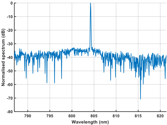
AlGaAs based lasers 68x nm to 8xxnm
AlGaAs based lasers 68x nm to 8xxnm Fabry-Perot and DFB lasers via re-growth MOCVD and MBE grown AlGaAs lasers spanning…
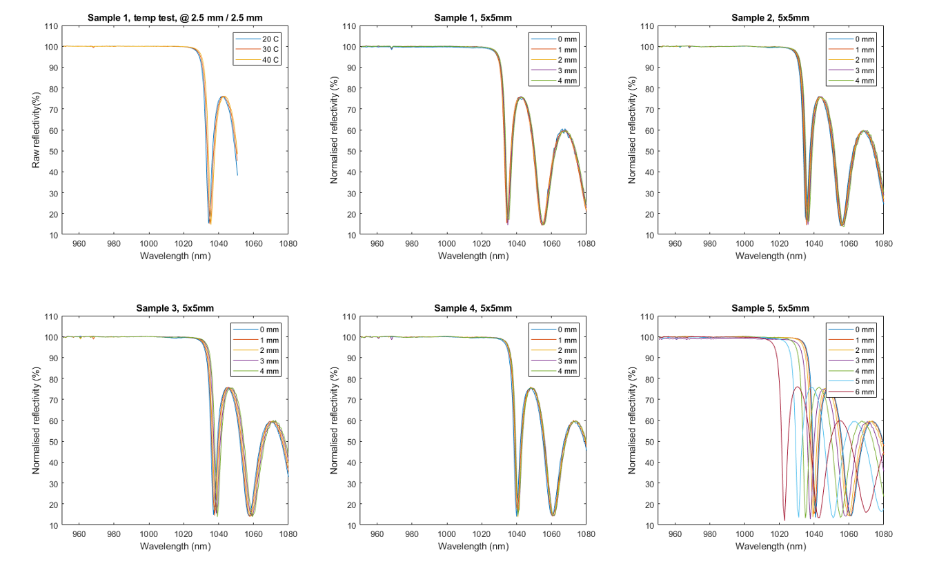
GaAs/AlAs DBRs – Wafer Mapping
~100% Reflectivity, & Excellent Uniformity MOCVD grown DBRs, developing our VECSEL technologies, were assessed in terms of wafer uniformity. Excellent…
Advanced InP Re-Growth
InP photonic crystal surface emitting laser (PCSEL) Very high aspect ratio features Significant experience and research in MOCVD epitaxial re-growth…
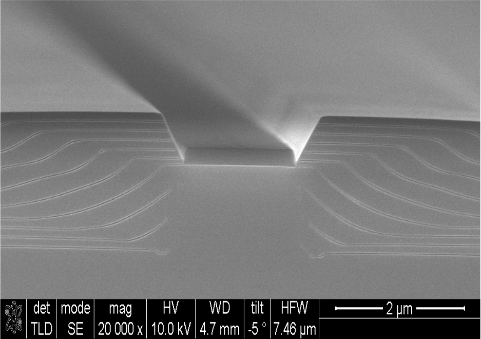
InP Buried-Heterostructures
This core MOCVD technology is applied to InP devices and PICs for engineering symmetric far-fields, ensuring efficient heat-extraction, and in…
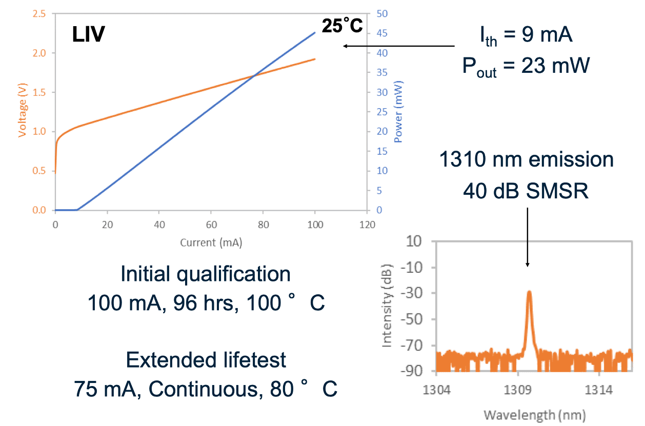
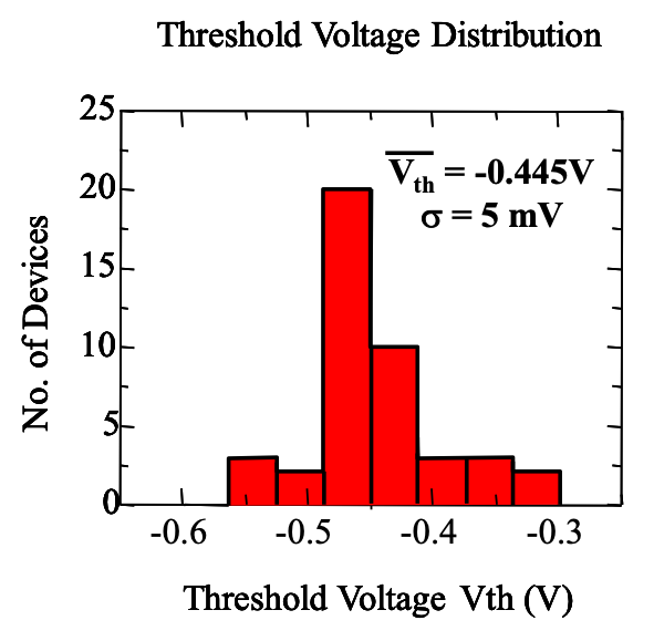
Qualified DFB – Test Data
Our InP DFB MOCVD re-growth processes have been qualified for commercial 1310nm DFBs.
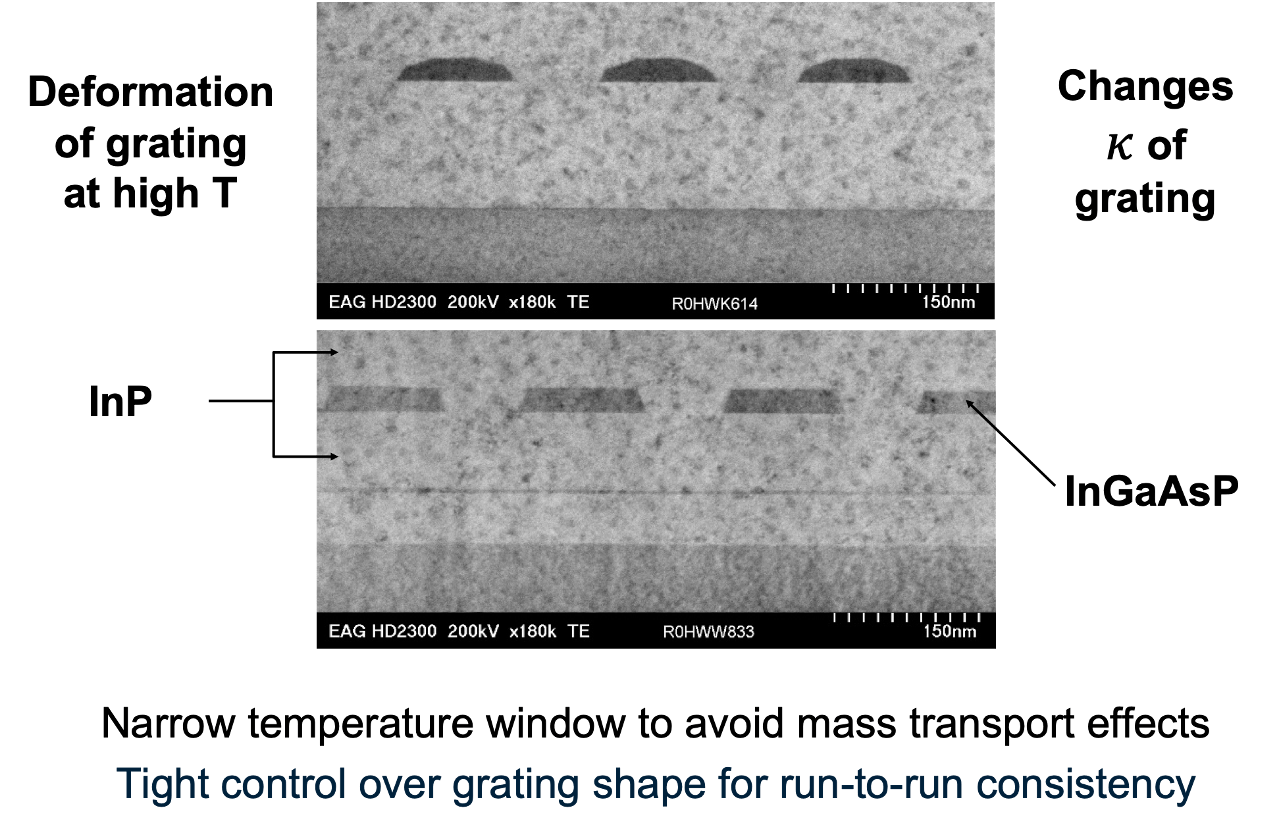
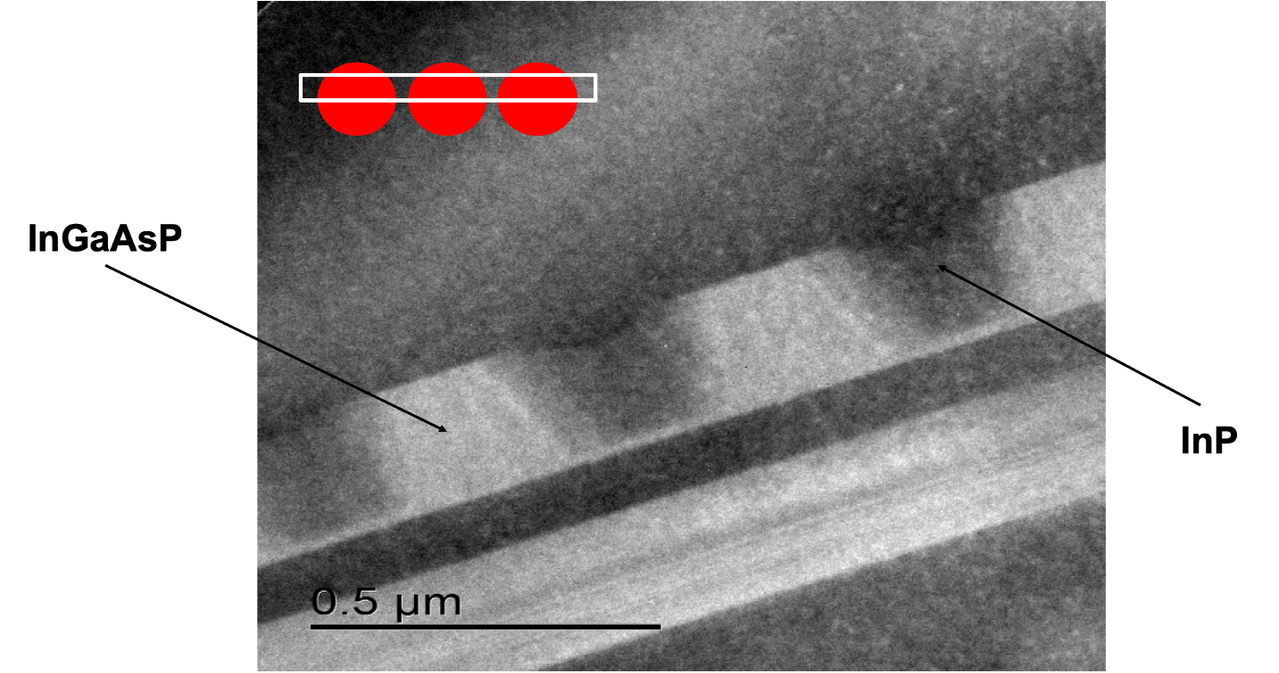
InP DFB Re-Growth
Iteration of MOCVD epitaxial re-growth, TEM structural characterisation, and device test of re-grown devices allows process development and transfer to…


Mid IR-DBRs
AlSb/GaInSb RCLED at ~4.25µm Broad area lasers have exhibited Jth=1.3 kAcm-2 In order to maximise extraction efficiency and engineer a…
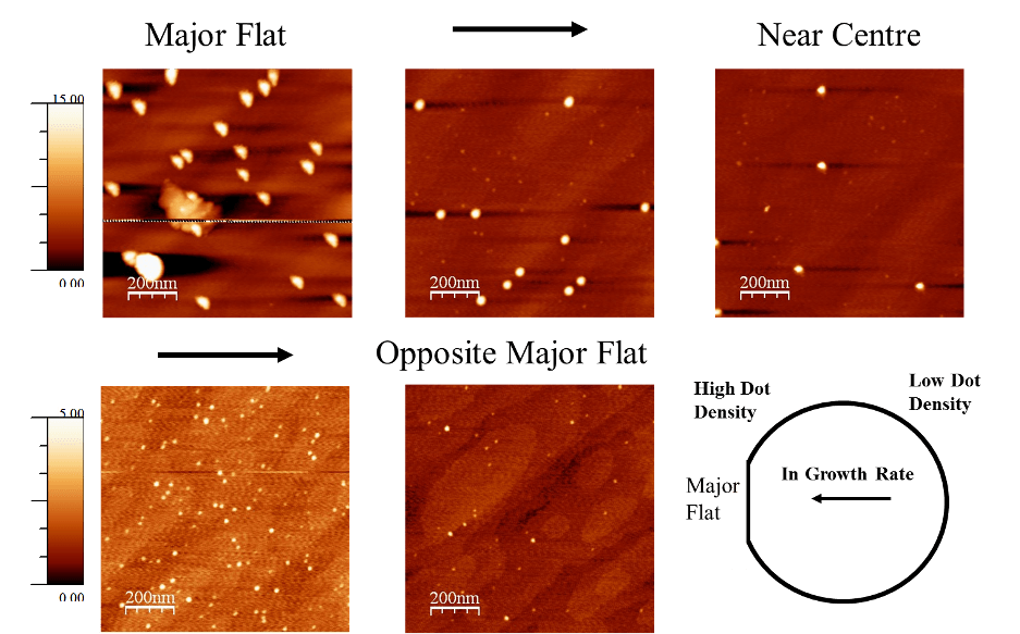
Low Density Quantum Dots
Single InAs QD required for physics studies Vary QD density across wafer by stopping rotation of wafer Phys. Rev. Lett.…
InSb Photo-Pixel & GaAs MESFET
AlInSb photo-detector GaAs MESFET GaAs substrate Xie, C., et al. (2015) . IEEE Transactions on Electron Devices, 62(12), pp. 4069-4075.…
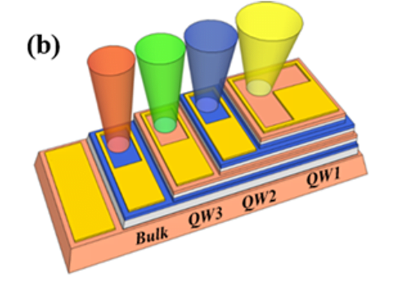
Multi-Spectral MIR LED
4x Colour MIR LED Grown on GaAs APL 111, (10), 102102. DOI: 10.1063/1.4986396 To allow future integration with GaAs based…
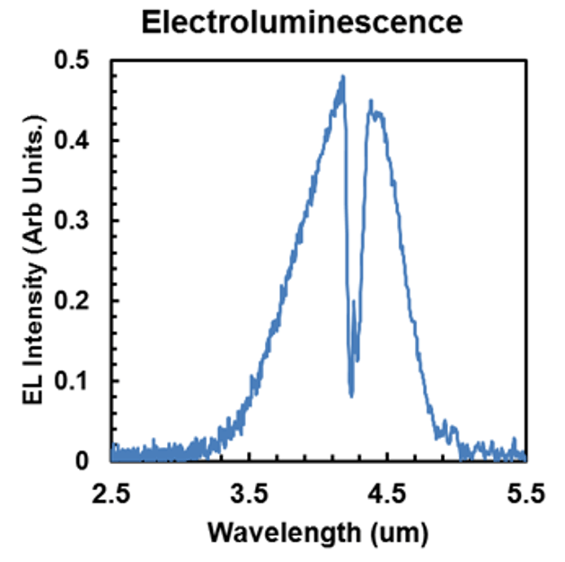
MIR LEDs & Photodiode – On Silicon
Full p-i-n structure grown on Si Electroluminescence ~4.25 μm III-V epitaxy on silicon processes have been developed to produce antimonide…
AlInGaAsSb Inter-band Lasers
Preliminary results – RT operation demonstrated With the R&D team of a leading laser manufacturer, we developed MBE epitaxial processes…

AlInGaAsSb Quantum Cascade Lasers
Development of QCL technologies in a range of projects through MBE grown base epitaxy.
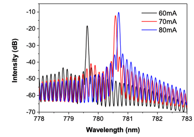
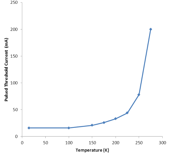
GaAs/AlGaAs Lasers (7xx–8xx nm)
Example: 780nm edge emitting laser structure Broad area lasers have exhibited Jth=1.3 kAcm-2

MBE Capabilities
VEECO GEN3 Systems Group III: Ga In and Al Group V : As, Sb, P Dopant : Si,Te (n), Be…
Call us today at +44 (0) 141 266 0115
or email us at info@iii-vepi.com
We look forward to hearing from you.