III-V Epi has the following MBE and MOCVD capabilities:
Current MBE and MOCVD tool configurations:
| Epitaxy Technology | Wafer Size | Alloys | Dopants | Epitaxy on Si? |
|---|---|---|---|---|
| MBE | 2-4” (50-100mm) | AlGaInAsSbP | Si, Te, Be | Yes – High Temperature Capability |
| MOCVD | 2-4” (50-100mm) | AlGaInAsP | Si, Zn, C, Fe | Yes – High Temperature Capability |
We have high resolution X-Ray Definition (XRD), Hall-effect, and eCV measurements that allow structural and electrical charactersiation, backed up by strong links to external partners for TEM, SIMS, etc.
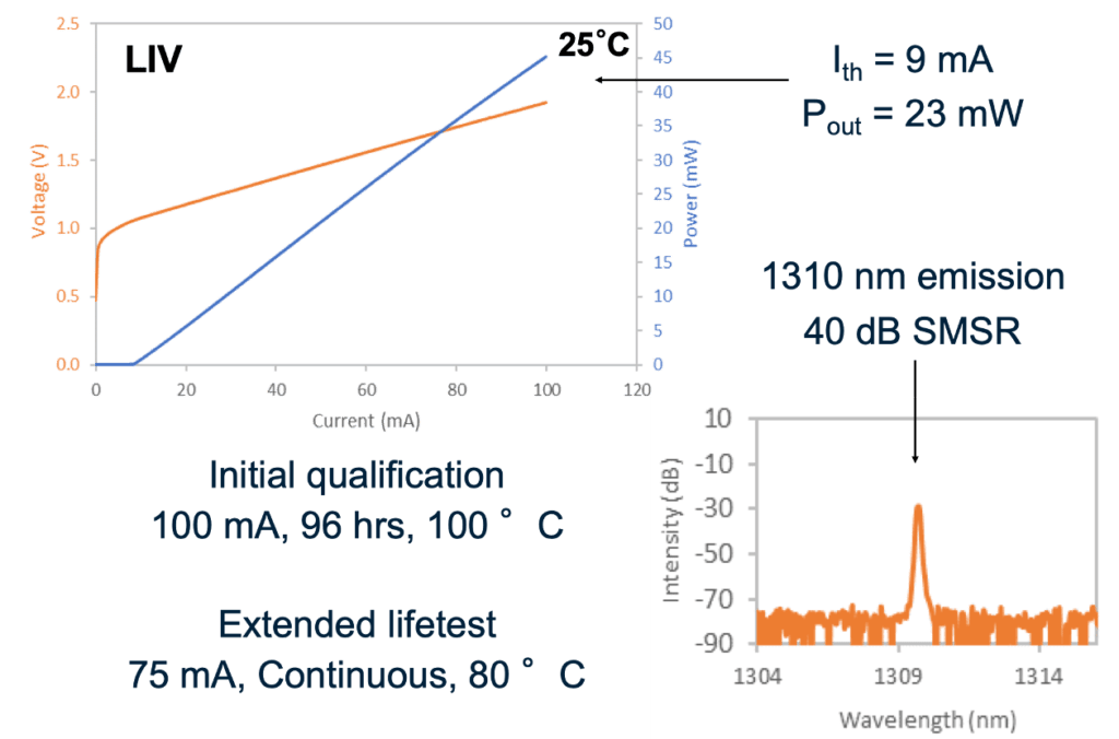
Our optical characterisation techniques span the UV to Mid-IR spectral ranges, with photoluminescence (PL) and reflectivity mapping, low temperature PL wafer mapping and micro-PL mapping.
We have a number of device-level metrology and charcaterisation test services available.
Our MBE capabilities:
Our equipment and material capabilities include:
- VEECO MBE Reactors
- Up to 4″ / 100mm
- Up to 1200C
- III-V on Silicon
- Group III : Ga, In, Al
- Group V : As, Sb, P
- Dopant : Si,Te (n), Be (p)
Our expertise includes:
- Sb based LEDs, LDs, PDs
- InP and GaAs HEMTs
- Quantum Cascade Lasers
- Quantum dot structures
Our MOCVD capabilities:
Our equipment and material capabilities include:
- Aixtron Reactors
- Up to 4″ / 100mm
- InP regrowth
- GaAs regrowth
- InGaAsP alloys
- AlGaAsInP alloys
Our expertise includes:
- Red-NIR (630-1700nm) LEDs, LDs, PDs
- GaAs based VCSELs, VECSELs
- Re-growth of InP and GaAs – DFBs, Buried Heterostructures, Selective Area Growth


Call us today at +44 (0) 141 266 0115
or email us at info@iii-vepi.com
We look forward to hearing from you.